With the rapid growth in AI hashrate demand, advanced process nodes and high-density chips have become the focal point of industry competition, significantly elevating the importance of semiconductor manufacturing. Equipment makers are no longer mere upstream suppliers; they are now pivotal forces that dictate the pace of process advancement and the ceiling on chip performance. As a result, Applied Materials' strategic role in the AI infrastructure cycle has been further reinforced.
From an industry perspective, the semiconductor equipment sector is undergoing a new wave of AI-driven capital expenditure. Ongoing fab expansions, growing demand for advanced packaging, and rising demand for high-bandwidth memory (HBM) are collectively boosting equipment investment intensity. As a multi-process platform provider, Applied Materials continues to broaden its product portfolio.
What Is Applied Materials (AMAT)? Company Background and Development History
Founded in 1967 and headquartered in the U.S., Applied Materials is a global leader in semiconductor and display equipment manufacturing. Initially specializing in materials engineering equipment, the company expanded into semiconductor deposition, etching, inspection, and packaging, building a comprehensive technology system that spans the entire wafer fabrication process.
As the semiconductor industry moved from micron-scale to nanometer-scale nodes, Applied Materials has consistently enhanced equipment precision and process capabilities through both strategic acquisitions and in-house R&D, securing a lasting leadership position in the advanced equipment market. Today, it serves as a key partner for fabs and chipmakers worldwide.
What Are Applied Materials' Core Business Segments?
Applied Materials' business is organized into three core segments: Semiconductor Systems, Applied Global Services, and Display and Adjacent Markets.
In semiconductors, the company offers deposition and etching equipment, ion implantation, and materials engineering solutions, serving logic chips, memory chips, and advanced process nodes.
In the display segment, Applied Materials supplies critical equipment for OLED and LCD panel production, commanding a substantial share in premium display manufacturing.
Additionally, its services segment—encompassing equipment maintenance, upgrades, and process optimization—fosters strong customer loyalty and a recurring revenue model.
How Semiconductor Equipment Drives AI and Advanced Process Development
The demand for hashrate from AI chips is pushing transistor density ever higher, a trend that depends on ongoing advances in process technology. Equipment makers are pivotal to this progression.
The deposition and etching tools from Applied Materials directly govern the precision and stability of transistor architectures. At 3nm, 2nm, and beyond, equipment accuracy emerges as a critical constraint on chip performance.
Moreover, the growing appetite for high-bandwidth memory (HBM) from AI data centers is raising the complexity of memory chip manufacturing, thereby boosting equipment demand.
Applied Materials' Core Technologies and Product Portfolio
Applied Materials' technology system is primarily centered around materials engineering and includes:
- Chemical Vapor Deposition (CVD)
- Physical Vapor Deposition (PVD)
- Atomic Layer Deposition (ALD)
- Dry etching and precision machining
Together, these technologies underpin the fundamental chip fabrication process, allowing transistor structures to be reliably built at nanometer scales.
Furthermore, the company has a presence in advanced packaging—including 3D stacking and heterogeneous integration—to meet the higher hashrate density requirements of AI chips.
Applied Materials' Role in Wafer Manufacturing, Advanced Packaging, and the Display Industry
In wafer fabrication, Applied Materials' tools are extensively deployed in logic and memory production lines, making the company a key supplier to leading fabs like TSMC, Samsung, and Intel.
In advanced packaging, the rise of chiplet architectures has pushed equipment demand beyond traditional wafer fabrication into packaging integration, thereby broadening the company's business scope.
In the display sector, high-precision manufacturing of OLED panels similarly depends on its materials engineering tools, with widespread application in premium smartphones and automotive displays.
How Does Applied Materials Differ from ASML, Lam Research, and KLA?
- ASML: Specializes in EUV lithography, the critical equipment supplier for the most advanced process nodes.
- Lam Research: Specializes in etching and thin-film deposition.
- KLA Corporation: Specializes in inspection and process control.
- Applied Materials: Covers deposition, materials engineering, and multi-process platform integration.
By contrast, Applied Materials' edge is its "end-to-end materials engineering capability" rather than a focus on any single process step, enabling deeper customer engagement across multiple nodes.
Key Risks to Seguir When Investing in AMAT Stock
While Applied Materials is a leader in the industry, investors should be aware of the following risks:
- The semiconductor industry is highly cyclical; fluctuations in capital spending can impact revenue stability.
- Geopolitical risks may affect global equipment exports and supply chain dynamics, particularly given heavy reliance on Asian markets.
- Rising R&D expenditures for advanced nodes and accelerating technology cycles may create periodic margin pressure.
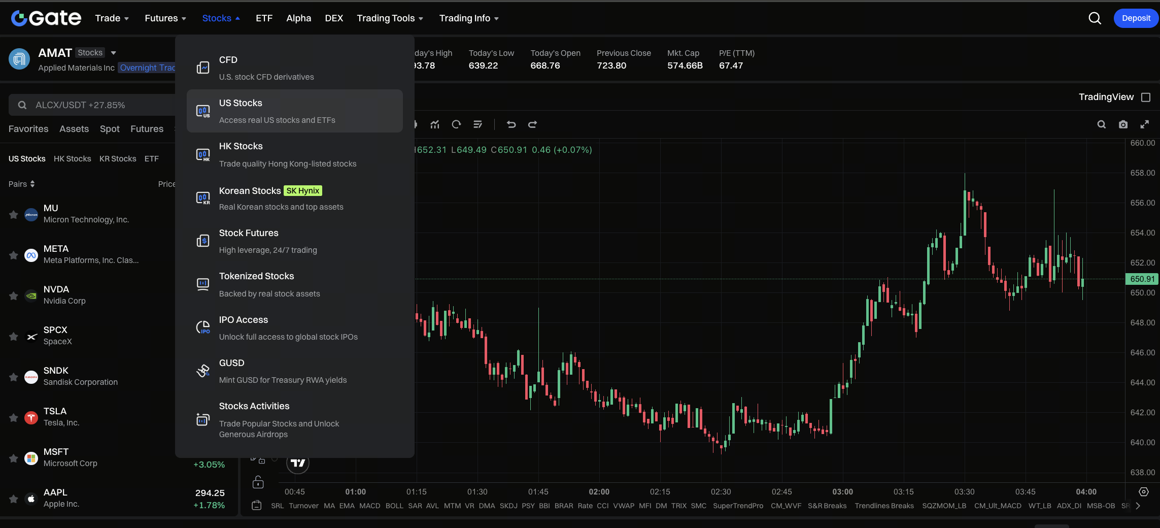
As investment and global asset allocation tools continue to evolve, some investors use multi-market trading platforms to track liquidity in semiconductor-related assets. For instance, Gate's stock trading service enables users to engage with price movements of U.S. and Hong Kong stocks within a single platform. With 24/7 trading and multi-asset connectivity, these platforms help mitigate the information lag associated with traditional trading hours, allowing investors to more flexibly monitor price changes and capital flows of semiconductor leaders like AMAT across different market sentiment cycles, ultimately enabling more efficient cross-market asset allocation and risk hedging.
Applied Materials' Future Outlook and Long-Term Growth Potential
Going forward, Applied Materials' growth is expected to be driven by three factors:
- Continued AI-driven process upgrades will sustain long-term equipment demand.
- Expansion of advanced packaging and chiplet architectures is broadening the application scope of equipment.
- Materials engineering is moving toward greater precision and lower energy consumption, underpinning the next wave of chip manufacturing.
With the ongoing expansion of AI infrastructure, the semiconductor equipment industry remains in a secular growth cycle, and Applied Materials is well-positioned to benefit from this structural demand.
Conclusion
As a global leader in semiconductor equipment, Applied Materials (AMAT) has established a comprehensive technology framework spanning wafer fabrication, advanced nodes, and materials engineering. With rising AI hashrate demands and ongoing chip process evolution, its central role in the global semiconductor supply chain continues to solidify. From both a technological and cyclical standpoint, Applied Materials remains on a long-term growth path.
FAQs
Q1: What does Applied Materials do?
It provides semiconductor manufacturing equipment, including deposition, etching, and materials engineering solutions.
Q2: What is the difference between AMAT and ASML?
ASML specializes in lithography equipment, whereas Applied Materials encompasses a wider scope of materials engineering and fabrication processes.
Q3: Is AMAT significantly impacted by AI?
Yes, significantly. AI chip demand directly drives investment in advanced nodes and equipment.
Q4: Is Applied Materials involved in advanced packaging?
Yes, the company is expanding its efforts in 3D packaging and heterogeneous integration.
Q5: What is the biggest risk in investing in AMAT?
Primarily the cyclical nature of semiconductors, along with global supply chain and geopolitical risks.