Unlike traditional packaging, advanced packaging is no longer just a "protective layer" for chips—it has become an integral part of chip performance. Through technologies such as Chiplet, 2.5D/3D stacking, and High Bandwidth Memory (HBM), computing units, memory units, and interconnect structures are being recombined, driving a shift from monolithic chip architectures to system-level integration. This transformation elevates packaging from a back-end process to a technology node as critical as the manufacturing process itself.
From an industry perspective, AI-driven demand for computing power is reshaping chip design and manufacturing logic. The traditional path of "improving performance with a single chip" is gradually hitting physical limits, making heterogeneous integration through advanced packaging the mainstream direction. In this process, the importance of equipment and materials technology has increased significantly. Applied Materials is deeply engaged in this structural transformation through materials engineering and packaging equipment capabilities.
What Is Advanced Packaging
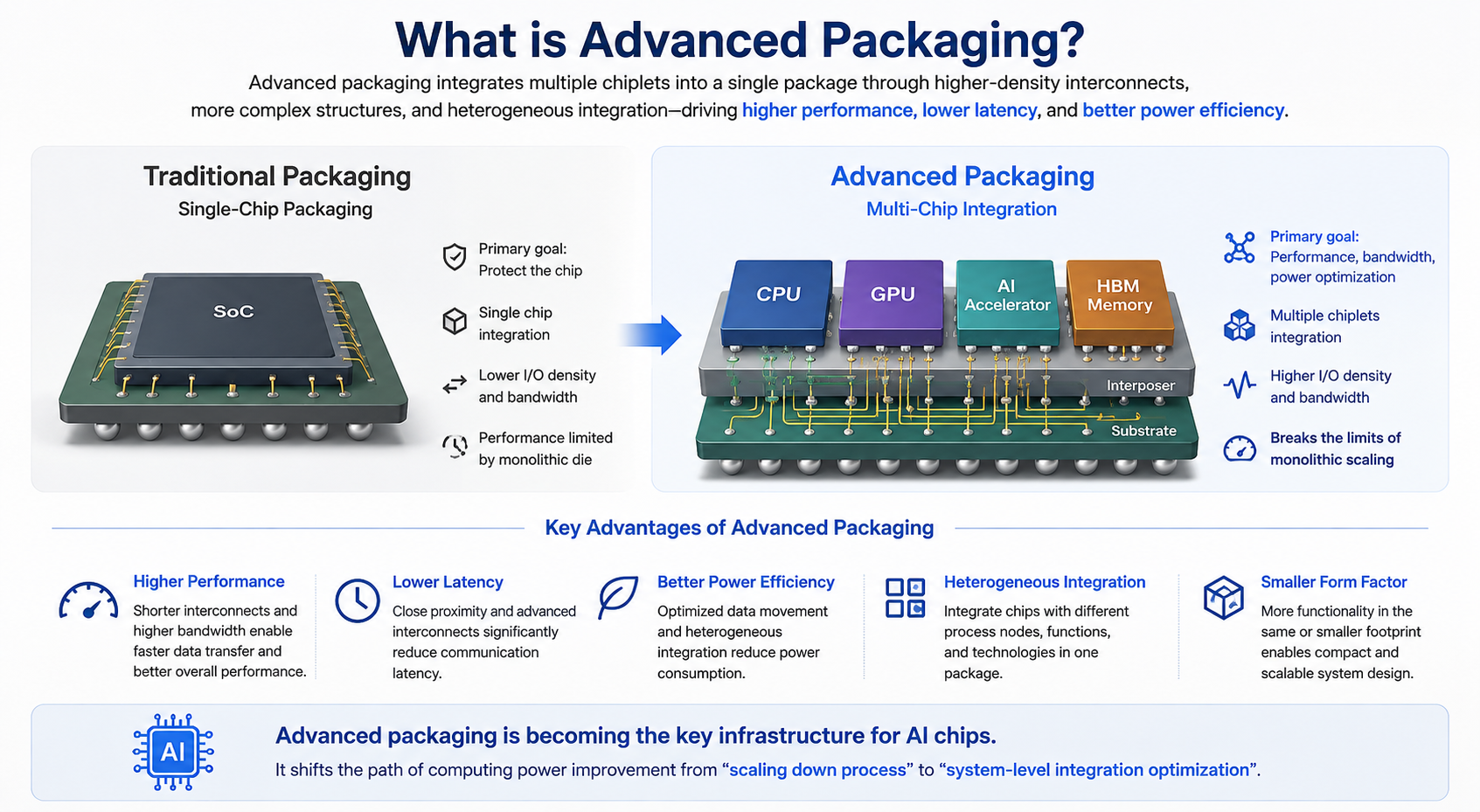
Advanced packaging refers to a technology system that integrates multiple chip functional modules into a single package using higher-density interconnects, more complex structural designs, and multi-chip integration methods. Unlike traditional packaging, its core goal is no longer simply to protect the chip, but to improve performance, reduce latency, and optimize power consumption.
Traditional packaging uses a single-chip packaging model, while advanced packaging enables multi-chip collaboration, allowing CPUs, GPUs, memory, and accelerators to connect under higher bandwidth conditions, thereby breaking through single-chip performance bottlenecks.
This technology is becoming a key infrastructure for AI chip development, shifting the path to increased computing power from "process node shrinking" to "system integration optimization."
How CoWoS, HBM, and Chiplet Are Changing Chip Manufacturing
In the advanced packaging ecosystem, CoWoS, HBM, and Chiplet architectures are the three core technology directions.
CoWoS (Chip on Wafer on Substrate) is a 2.5D packaging technology that integrates multiple chips on the same substrate via an interposer, enabling high-speed interconnects. This structure is widely used in AI GPUs and high-performance computing chips.
HBM (High Bandwidth Memory) significantly increases memory bandwidth through vertical stacking, allowing AI model training to handle larger data throughput requirements.
The Chiplet architecture further changes chip design logic by splitting a single large chip into multiple functional modules and combining them through advanced packaging, thereby improving yield and reducing manufacturing costs.
Together, these three technologies drive chip manufacturing from "monolithic structures" toward "modular systems."
How Applied Materials Is Positioning Its Advanced Packaging Equipment
In the field of advanced packaging, Applied Materials is extending its materials engineering capabilities to the packaging level.
The company supports the manufacturing needs of 3D stacking, heterogeneous integration, and high-density interconnect structures by providing high-precision deposition and etching equipment. These tools are used to build key structures such as micro bumps, RDL (redistribution layer), and TSV (through-silicon vias).
In addition, Applied Materials is developing dedicated materials engineering solutions for advanced packaging to enhance packaging reliability and thermal management. This positioning allows the company to gradually expand from a traditional wafer equipment supplier into a system-level manufacturing solution provider.
Why Materials Engineering Is Critical in Advanced Packaging
The complexity of advanced packaging lies not only in structural design but also in material selection and interface control.
In high-density integration environments, differences in thermal expansion coefficients, conductivity, and mechanical stress among different chips directly affect stability. Therefore, materials engineering becomes a key factor determining packaging reliability.
By optimizing dielectric materials, thermal interface materials, and metal interconnect structures, packaging performance and lifespan can be significantly improved. This is also a key competitive advantage for Applied Materials in this field.
The stronger the materials engineering capability, the more complex 3D integration structures it can support, thereby enabling higher computing power density.
Why AI Chips Are Driving Growth in Advanced Packaging Demand
AI chips require far more computing power and bandwidth than traditional chips, as their training and inference processes involve handling massive datasets and high-frequency computing tasks.
Single-chip performance improvement has gradually approached physical limits, prompting the industry to turn to advanced packaging for system-level performance gains.
The combination of HBM and GPUs makes memory bandwidth a bottleneck, and advanced packaging effectively addresses this by shortening chip distances and increasing interconnect speeds.
Meanwhile, the rapid expansion of AI data centers further amplifies packaging demand, making advanced packaging an investment direction as important as the manufacturing process itself.
How Applied Materials Differs from BE Semiconductor and ASMPT
In the advanced packaging equipment space, different vendors have different focuses:
BE Semiconductor Industries specializes in advanced packaging assembly and bonding equipment, excelling particularly in die attach and hybrid bonding;
ASMPT covers packaging and surface mount equipment, with a strong market share in traditional packaging and some areas of advanced packaging;
In contrast, Applied Materials' strength lies in materials engineering and front-to-back-end process integration, rather than being limited to packaging assembly.
This difference positions it closer to a "foundational process platform provider," capable of participating in the core manufacturing processes of advanced packaging rather than simply offering equipment tools.
What Challenges Does the Advanced Packaging Industry Face
Advanced packaging is growing rapidly but faces multiple challenges. Technical complexity has increased significantly, and multi-chip integration brings higher yield control difficulty. Thermal management issues have become more prominent, with high-density integration leading to greater heat dissipation pressure. Supply chain complexity raises manufacturing costs and imposes stricter requirements on equipment precision and material consistency. Inconsistent chip design standards further increase packaging integration difficulty.
Future Development Directions of Advanced Packaging Technology
Advanced packaging will continue to evolve along three directions.
-
3D stacking technology will further mature, achieving higher vertical integration density.
-
Chiplet standardization will accelerate, enhancing compatibility between chips from different manufacturers.
-
Materials science and packaging processes will further integrate, significantly improving thermal management and signal integrity.
Against the backdrop of sustained AI-driven computing power demand, advanced packaging will gradually become the main battleground for chip performance optimization.
Summary
Advanced packaging is transforming from a traditional back-end process into a core component of chip performance. CoWoS, HBM, and Chiplet architectures together drive the evolution of chips from monolithic designs to system-level integration. In this trend, Applied Materials, through materials engineering and equipment capabilities, is deeply involved in industrial upgrading, becoming an important technology platform connecting wafer manufacturing and system integration. As AI computing power demand continues to grow, advanced packaging will become a key competitive frontier in the next phase of the semiconductor industry.