As chip fabrication moves into 3nm, 2nm, and beyond, the conventional reliance on geometric scaling to boost performance is hitting physical boundaries. The industry is now pivoting toward material-driven innovation. Differences in electrical conductivity, thermal stability, and quantum effects across various materials are directly influencing transistor performance and energy efficiency, elevating materials engineering from a supporting function to a core technological pathway.
From an industry standpoint, the explosive growth in AI computing demand is accelerating this shift. High Bandwidth Memory, heterogeneous computing, and advanced packaging technologies are converging, significantly raising the complexity of chip systems. In this context, materials engineering doesn't just affect individual transistors—it defines the performance ceiling of entire system-on-chip (SoC) designs.
What Is Materials Engineering
Materials engineering is the discipline of studying and designing the structure, properties, and processing of materials. In semiconductors, it focuses on optimizing transistor materials, dielectric layers, conductive layers, and interface architectures.
In chip manufacturing, materials engineering goes beyond "which material to use"—it encompasses "how to precisely control material arrangement at the nanoscale." This directly impacts a chip's conductive efficiency, power consumption, and stability.
As chip dimensions shrink, material properties increasingly become performance bottlenecks. Phenomena like quantum tunneling, thermal diffusion, and rising resistance are forcing the industry to continuously explore new materials and structural solutions.
Why Advanced Nodes Increasingly Rely on New Materials
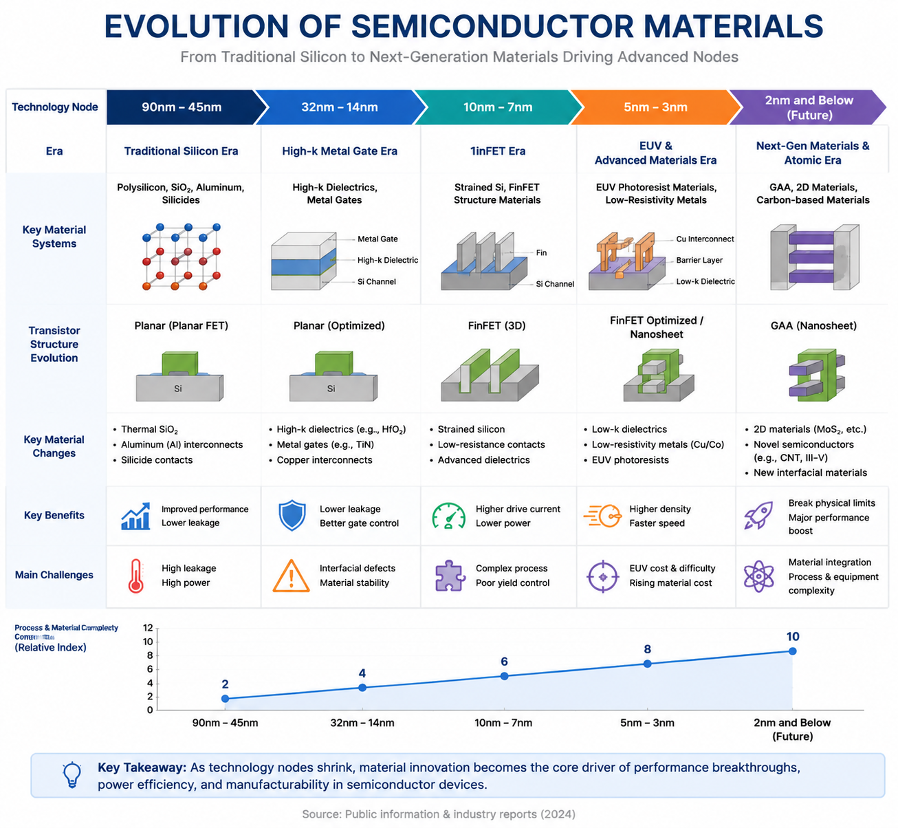
The focus of advanced process development has shifted from "shrinking transistor size" to "changing material structure." Traditional silicon-based materials are showing performance limits at extreme dimensions, necessitating the adoption of high-k dielectrics, metal gates, and new conductive materials. At 3nm and below, transistor architectures have moved from planar to FinFET and even GAA (Gate-All-Around) structures, imposing stricter material requirements.
New materials not only boost performance—they also lower power consumption and improve yield, enabling stable operation at higher frequencies.
Applied Materials delivers nanoscale precision in transistor fabrication through deposition, etching, and materials engineering. During deposition, its equipment creates ultra-thin, uniform material layers that form the transistor's structural foundation. In etching, high-precision processing removes excess material to shape complex circuit patterns.
Additionally, the company's advances in Atomic Layer Deposition (ALD) allow materials to be built atomic layer by atomic layer, dramatically improving transistor consistency and performance stability. Together, these technologies enhance manufacturing efficiency and yield for advanced nodes, making them critical to high-volume production of leading-edge chips.
How Materials Innovation Fuels AI Chip Development
AI chips demand extreme hashrate density and energy efficiency—metrics heavily tied to material performance. In GPUs and AI ASICs, materials determine transistor switching speed and power consumption, while also affecting chip-to-chip interconnect efficiency.
The widespread adoption of High Bandwidth Memory (HBM) further raises the bar, requiring lower-resistance interconnects and higher-thermal-conductivity materials to support dense data transfers.
Materials innovation is directly steering AI chips from a "raw compute growth" mindset toward "system-level efficiency optimization."
Applied Materials' Role in Logic, Memory, and Advanced Packaging
In logic, Applied Materials' equipment builds advanced transistor structures, including the critical material layers for FinFET and GAA architectures.
In memory, its technologies enable higher stacking densities in NAND and DRAM, boosting storage capacity and performance.
In advanced packaging, the company is extending its materials engineering expertise into 2.5D and 3D integration, supporting Chiplet architectures and heterogeneous computing.
This end-to-end positioning transforms it from a pure equipment vendor into a system-level materials solution provider.
How Applied Materials Stands Apart from Traditional Equipment Makers
Traditional semiconductor equipment makers typically focus on a single process step. Applied Materials' key differentiator is its "materials platform capability." For instance, ASML specializes in lithography, Lam Research in etching, while Applied Materials spans deposition, etching, and materials engineering across multiple steps.
This cross-process integration allows it to influence the entire chip fabrication flow at the material level, rather than supplying just one piece of equipment.
Opportunities and Challenges in the Materials Engineering Landscape
Materials engineering is growing rapidly, but it faces multiple challenges.
Opportunities: The AI chip boom, steady advancement of process nodes, and the spread of advanced packaging are all expanding the materials engineering market.
Challenges: Long R&D cycles, complex technology validation, and extreme equipment precision requirements.
Moreover, new materials must be compatible with existing manufacturing processes, adding to the difficulty of commercialization.
Future Directions for Applied Materials' Technology
The future of materials engineering will focus on several key areas.
-
Atomic-scale manufacturing will mature, enabling even finer material control.
-
Low-power and high-thermal-conductivity materials will become research priorities to address AI chip cooling challenges.
-
Deeper integration of materials and advanced packaging will further boost SoC performance.
-
AI-driven materials discovery (Materials AI) may accelerate the identification and validation of new materials.
Driven by these trends, Applied Materials' platform strengths will only grow.
Summary
Materials engineering is emerging as one of the most critical innovation drivers in semiconductors, with importance rivaling transistor design itself. As AI chip complexity climbs, material choices and structural design directly set the upper limits of chip performance.
Through deposition, etching, and materials engineering, Applied Materials has built a comprehensive capability spanning wafer fabrication and advanced packaging, securing a central position in the semiconductor supply chain. In the AI-driven long-term growth cycle, materials engineering will remain the foundational engine powering chip performance evolution.